SBOS656C July 2016 – December 2016 INA260
PRODUCTION DATA.
- 1 Features
- 2 Applications
- 3 Description
- 4 Revision History
- 5 Related Products
- 6 Pin Configuration and Functions
- 7 Specifications
-
8 Detailed Description
- 8.1 Overview
- 8.2 Functional Block Diagram
- 8.3 Feature Description
- 8.4 Device Functional Modes
- 8.5 Programming
- 8.6
Register Maps
- 8.6.1 Configuration Register (00h) (Read/Write)
- 8.6.2 Current Register (01h) (Read-Only)
- 8.6.3 Bus Voltage Register (02h) (Read-Only)
- 8.6.4 Power Register (03h) (Read-Only)
- 8.6.5 Mask/Enable Register (06h) (Read/Write)
- 8.6.6 Alert Limit Register (07h) (Read/Write)
- 8.6.7 Manufacturer ID Register (FEh) (Read-Only)
- 8.6.8 Die ID Register (FFh) (Read-Only)
- 9 Application and Implementation
- 10Power Supply Recommendations
- 11Layout
- 12Device and Documentation Support
- 13Mechanical, Packaging, and Orderable Information
Package Options
Mechanical Data (Package|Pins)
- PW|16
Thermal pad, mechanical data (Package|Pins)
Orderable Information
1 Features
- Precision Integrated Shunt Resistor:
- Current Sense Resistance: 2 mΩ
- Tolerance Equivalent to 0.1%
- 15-A Continuous From –40°C to +85°C
- 10 ppm/°C Temperature Coefficient
(0°C to +125°C )
- Senses Bus Voltages From 0 V to 36 V
- High-Side or Low-Side Sensing
- Reports Current, Voltage, and Power
- High Accuracy:
- 0.15% System Gain Error (Maximum)
- 5-mA Offset (Maximum)
- Configurable Averaging Options
- 16 Programmable Addresses
- Operates From a 2.7-V to 5.5-V Power Supply
- 16-Pin, TSSOP Package
2 Applications
- Test Equipment
- Servers
- Telecom Equipment
- Computing
- Power Management
- Battery Chargers
- Power Supplies
3 Description
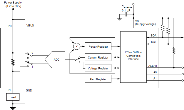
The INA260 is a digital-output, current, power, and voltage monitor with an I2C and SMBus™-compatible interface with an integrated precision shunt resistor. It enables high-accuracy current and power measurements and over-current detection at common-mode voltages that can vary from 0 V to 36 V, independent of the supply voltage. The device is a bidirectional, low- or high-side, current-shunt monitor that measures current flowing through the internal current-sensing resistor. The integration of the precision current-sensing resistor provides calibration-equivalent measurement accuracy with ultra-low temperature drift performance and ensures that an optimized Kelvin layout for the sensing resistor is always obtained.
The INA260 features up to 16 programmable addresses on the I2C-compatible interface. The digital interface allows programmable alert thresholds, analog-to-digital converter (ADC) conversion times, and averaging. To facilitate ease of use, an internal multiplier enables direct readouts of current in amperes and power in watts.
The device operates from a single 2.7-V to 5.5-V supply, drawing 310 μA (typical) of supply current. The INA260 is specified over the operating temperature range between –40°C and +125°C and is available in the 16-pin TSSOP package.
Device Information(1)
| PART NUMBER | PACKAGE | BODY SIZE (NOM) |
|---|---|---|
| INA260 | TSSOP (16) | 5.00 mm x 4.40 mm |
- For all available packages, see the orderable addendum at the end of the datasheet.
High-Side Sensing Application
