SBOS558C April 2011 – April 2016 INA200-Q1 , INA201-Q1 , INA202-Q1
PRODUCTION DATA.
- 1 Features
- 2 Applications
- 3 Description
- 4 Revision History
- 5 Device Comparison Table
- 6 Pin Configuration and Functions
- 7 Specifications
- 8 Parameter Measurement Information
- 9 Detailed Description
- 10Application Information
- 11Power Supply Recommendations
- 12Layout
- 13Device and Documentation Support
- 14Mechanical, Packaging, and Orderable Information
Package Options
Mechanical Data (Package|Pins)
- DGK|8
Thermal pad, mechanical data (Package|Pins)
Orderable Information
1 Features
- Qualified for Automotive Applications
- AEC-Q100 Qualified With the Following Results:
- Current-Sense Amplifier:
- Common-Mode Range: –16 V to +80 V
- 3.5% Max Error Over Temperature
- Bandwidth: 500 kHz (INA200-Q1)
- Three Gain Options:
- 20 V/V (INA200-Q1)
- 50 V/V (INA201-Q1)
- 100 V//V (INA202-Q1)
- Integrated Open-Drain Comparator
- Latching Capability
- 0.6-V Internal Voltage Reference
- Quiescent Current: 1800 μA (Max)
- Latch-Up Exceeds 100 mA per JESD78
- Package: VSSOP-8
2 Applications
3 Description
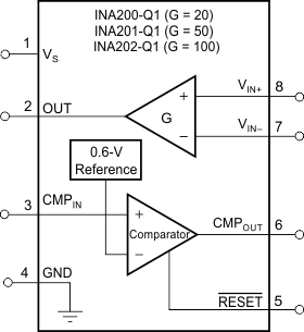
The INA200-Q1, INA201-Q1, and INA202-Q1 (INA20x-Q1) are low- or high-side current-shunt monitors with voltage output. The INA20x-Q1 devices can sense drops across shunts at common-mode voltages from –16 V to +80 V. The INA20x-Q1 are available with three output voltage scales: 20 V/V, 50 V/V, and 100 V/V, with up to a 500-kHz bandwidth.
The INA20x-Q1 also incorporate an open-drain comparator and internal reference that provides a 0.6-V threshold. External dividers set the current trip point. The comparator includes a latching capability, and can be made transparent by grounding (or leaving open) the RESET pin.
The INA20x-Q1 operate from a single 2.7-V to 18-V supply, drawing a maximum of 1800 μA of supply current. These devices are available in the very small VSSOP-8 package. Specifications for all devices extend over the operating temperature range of –40°C to +125°C.
Device Information(1)
| PART NUMBER | PACKAGE | BODY SIZE (NOM) |
|---|---|---|
| INA200-Q1 | VSSOP (8) | 3.00 mm x 3.00 mm |
| INA201-Q1 | ||
| INA202-Q1 |
- For all available packages, see the package option addendum at the end of the data sheet.
