SLVSCX2B August 2015 – February 2016 DRV8305
PRODUCTION DATA.
- 1 Features
- 2 Applications
- 3 Description
- 4 Revision History
- 5 Pin Configuration and Functions
- 6 Specifications
-
7 Detailed Description
- 7.1 Overview
- 7.2 Functional Block Diagram
- 7.3
Feature Description
- 7.3.1 Integrated Three-Phase Gate Driver
- 7.3.2 INHx/INLx: Gate Driver Input Modes
- 7.3.3 VCPH Charge Pump: High-Side Gate Supply
- 7.3.4 VCP_LSD LDO: Low-Side Gate Supply
- 7.3.5 GHx/GLx: Half-Bridge Gate Drivers
- 7.3.6 DVDD and AVDD: Internal Voltage Regulators
- 7.3.7 VREG: Voltage Regulator Output
- 7.3.8 Protection Features
- 7.3.9 Undervoltage Warning (UVFL), Undervoltage Lockout (UVLO), and Overvoltage (OV) Protection
- 7.4 Device Functional Modes
- 7.5 Programming
- 7.6
Register Maps
- 7.6.1 Status Registers
- 7.6.2
Control Registers
- 7.6.2.1 HS Gate Drive Control (Address = 0x5)
- 7.6.2.2 LS Gate Drive Control (Address = 0x6)
- 7.6.2.3 Gate Drive Control (Address = 0x7)
- 7.6.2.4 IC Operation (Address = 0x9)
- 7.6.2.5 Shunt Amplifier Control (Address = 0xA)
- 7.6.2.6 Voltage Regulator Control (Address = 0xB)
- 7.6.2.7 VDS Sense Control (Address = 0xC)
- 8 Application and Implementation
- 9 Power Supply Recommendations
- 10Layout
- 11Device and Documentation Support
- 12Mechanical, Packaging, and Orderable Information
Package Options
Mechanical Data (Package|Pins)
- PHP|48
Thermal pad, mechanical data (Package|Pins)
- PHP|48
Orderable Information
1 Features
- 4.4-V to 45-V Operating Voltage
- 1.25-A and 1-A Peak Gate Drive Currents
- Programmable High- and Low-Side Slew-Rate Control
- Charge-Pump Gate Driver for 100% Duty Cycle
- Three Integrated Current-Shunt Amplifiers
- Integrated 50-mA LDO (3.3-V and 5-V Option)
- 3-PWM or 6-PWM Input Control up to 200 kHz
- Single PWM-Mode Commutation Capability
- Supports Both 3.3-V and 5-V Digital Interface
- Serial Peripheral Interface (SPI) for Device Settings and Fault Reporting
- Thermally-Enhanced 48-Pin HTQFP
- Protection Features:
- Fault Diagnostics and MCU Watchdog
- Programmable Dead-Time Control
- MOSFET Shoot-Through Prevention
- MOSFET VDS Overcurrent Monitors
- Gate-Driver Fault Detection
- Reverse Battery-Protection Support
- Limp Home-Mode Support
- Overtemperature Warning and Shutdown
2 Applications
- Three-Phase BLDC and PMSM Motors
- CPAP and Pumps
- Robotics and RC Toys
- Power Tools
- Industrial Automation
3 Description
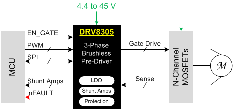
The DRV8305 device is a gate driver IC for three-phase motor-drive applications. The device provides three high-accuracy and temperature compensated half-bridge drivers, each capable of driving a high-side and low-side N-channel MOSFET. A charge pump driver supports 100% duty cycle and low-voltage operation. The device can tolerate load dump voltages up to 45-V.
The DRV8305 device includes three bidirectional current-shunt amplifiers for accurate low-side current measurements that support variable gain settings and an adjustable offset reference.
The DRV8305 device has an integrated voltage regulator (3.3-V or 5-V) to support an MCU or other system power requirements. The voltage regulator can be interfaced directly with a standard LIN physical interface to allow low system standby and sleep currents.
The gate driver uses automatic handshaking when switching to prevent current shoot through. The VDS of both the high-side and low-side MOSFETs is accurately sensed to protect the external MOSFETs from overcurrent conditions. The SPI provides detailed fault reporting, diagnostics, and device configurations such as gain options for the current shunt amplifier, individual MOSFET overcurrent detection, and gate-drive slew-rate control.
Device Options:
- DRV8305N: Voltage reference
- DRV83053: 3.3-V, 50-mA LDO
- DRV83055: 5-V, 50-mA LDO
Device Information (1)
| PART NUMBER | PACKAGE | BODY SIZE (NOM) |
|---|---|---|
| DRV8305 | HTQFP (48) | 7.00 mm × 7.00 mm |
- For all available packages, see the orderable addendum at the end of the data sheet.
Simplified Schematic
