DLPS023C January 2012 – August 2015 DLPC300
PRODUCTION DATA.
- 1 Features
- 2 Applications
- 3 Description
- 4 Revision History
- 5 Pin Configuration and Functions
-
6 Specifications
- 6.1 Absolute Maximum Ratings
- 6.2 ESD Ratings
- 6.3 Recommended Operating Conditions
- 6.4 Thermal Information
- 6.5 I/O Electrical Characteristics
- 6.6 Crystal Port Electrical Characteristics
- 6.7 Power Consumption
- 6.8 I2C Interface Timing Requirements
- 6.9 Parallel Interface Frame Timing Requirements
- 6.10 Parallel Interface General Timing Requirements
- 6.11 Parallel I/F Maximum Supported Horizontal Line Rate
- 6.12 BT.565 I/F General Timing Requirements
- 6.13 Flash Interface Timing Requirements
- 6.14 DMD Interface Timing Requirements
- 6.15 Mobile Dual Data Rate (mDDR) Memory Interface Timing Requirements
- 6.16 JTAG Interface: I/O Boundary Scan Application Switching Characteristics
- 7 Detailed Description
-
8 Application and Implementation
- 8.1 Application Information
- 8.2 Typical Application
- 8.3 System Examples
- 9 Power Supply Recommendations
-
10Layout
- 10.1
Layout Guidelines
- 10.1.1 Printed Circuit Board Design Guidelines
- 10.1.2 Printed Circuit Board Layer Stackup Geometry
- 10.1.3 Signal Layers
- 10.1.4 Routing Constraints
- 10.1.5 Termination Requirements
- 10.1.6 PLL
- 10.1.7 General Handling Guidelines for Unused CMOS-Type Pins
- 10.1.8 Hot-Plug Usage
- 10.1.9 External Clock Input Crystal Oscillator
- 10.2 Layout Example
- 10.3 Thermal Considerations
- 10.1
Layout Guidelines
- 11Device and Documentation Support
- 12Mechanical, Packaging, and Orderable Information
Package Options
Refer to the PDF data sheet for device specific package drawings
Mechanical Data (Package|Pins)
- ZVB|176
Thermal pad, mechanical data (Package|Pins)
Orderable Information
1 Features
- Required for Reliable Operation of the DLP3000 DMD
- Multi-Mode, 24-Bit Input Port:
- Supports Parallel RGB With Pixel Clock Up to 33.5 MHz and 3 Input Color Bit-Depth Options:
- 24-Bit RGB888 or 4:4:4 YCrCb888
- 18-Bit RGB666 or 4:4:4 YCrCb666
- 16-Bit RGB565 or 4:2:2 YCrCb565
- Supports 8-Bit BT.656 Bus Mode With Pixel Clock Up to 33.5 MHz
- Supports Parallel RGB With Pixel Clock Up to 33.5 MHz and 3 Input Color Bit-Depth Options:
- Supports Input Resolutions 608 × 684, 864 × 480, 854 × 480 (WVGA), 640 × 480 (VGA), 320 × 240 (QVGA)
- Pattern Input Mode
- One-to-One Mapping of Input Data to Micromirrors
- 1-Bit Binary Pattern Rates up to 4000-Hz
- 8-Bit Grayscale Pattern Rates up to 120-Hz
- Video Input Mode with Pixel Data Processing
- Supports 1- to 60-Hz Frame Rates
- Programmable Degamma
- Spatial-Temporal Multiplexing (Dithering)
- Automatic Gain Control
- Color Space Conversion
- Output Trigger Signal for Synchronizing With Camera, Sensor, or Other Peripherals
- System Control:
- I2C Control of Device Configuration
- Programmable Current Control of up to 3 LEDs
- Integrated DMD Reset Driver Control
- DMD Horizontal and Vertical Display Image Flip
- Low-Power Consumption: Less than 93 mW (Typical)
- External Memory Support:
- 166-MHz Mobile DDR SDRAM
- 33.3-MHz Serial FLASH
- 176-Pin, 7 × 7 mm With 0.4-mm Pitch NFBGA Package
2 Applications
- 3D Metrology
- 3D Scanning
- Factory Automation
- Fingerprint Identification
- Fringe Projection
- Industrial In line Inspection
- Robotic Vision
- Stereoscopic Vision
- Chemical Sensing
- Mobile Sensing
- Spectroscopy
- Augmented Reality
- Information Overlay
- Medical Instruments
- Virtual Gauges
3 Description
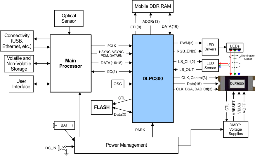
The DLPC300 controller provides a convenient, multi-functional interface between user electronics and the DMD, enabling high-speed pattern rates (up to 4-kHz binary), providing LED control, and data formatting for multiple input resolutions. The DLPC300 digital controller, part of the DLP3000 chipset, is required for reliable operation of the DLP3000 DMD. The DLPC300 also outputs a trigger signal for synchronizing displayed patterns with a camera, sensor, or other peripherals.
Device Information(1)
| PART NUMBER | PACKAGE | BODY SIZE (NOM) |
|---|---|---|
| DLPC300 | NFBGA (176) | 7.00 mm × 7.00 mm |
- For all available packages, see the orderable addendum at the end of the data sheet.
4 Revision History
Changes from B Revision (July 2013) to C Revision
- Added ESD Ratings table, Feature Description section, Device Functional Modes, Application and Implementation section, Power Supply Recommendations section, Layout section, Device and Documentation Support section, and Mechanical, Packaging, and Orderable Information section Go
- Added active low to MEM_RAS, MEM_CAS, and MEM_CS in Figure 7Go
Changes from A Revision (July 2012) to B Revision
- Changed GPIO4_INF to INIT_DONEGo
- Deleted “RESERVED0” and “RESERVED1” rows in Go
- Deleted “d” from Terminal No. R12 in Go
- Changed pin name GPIO4_INTF to INIT_DONEGo
- Changed INIT_DONE (formerly GPIO4_INTF) pin descriptionGo
- Changed pin name GPIO0_CMPPWR to CMP_PWRGo
- Changed pin name JTAGRSTZ to JTAGRSTGo
- Changed the "Reserved" row information in Go
- Changed Note 1 From: "6 total reserved pins" To: "7 total reserved pins" Go
- Added video mode non-linear gamma correction descriptionGo
- Added structured light mode linear gamma descriptionGo
- Added DDR DRAM devices to Table 6Go
- Changed GPIO4_INTF to INIT_DONEGo
- Changed GPIO4_INTF to INIT_DONEGo
- Changed GPIO4_INTF to INIT_DONEGo
- Changed GPIO4 to INIT_DONEGo
Changes from * Revision (January 2012) to A Revision
- Changed Features Item From: Supports Input Resolutions 608 × 684, 854 × 480 (WVGA), 640 × 480 (VGA), 320 × 240 (QVGA) To: Supports Input Resolutions 608 × 684, 864 × 480, 854 × 480 (WVGA), 640 × 480 (VGA), 320 × 240 (QVGA)Go
- Changed unit values from ms to µs in I2C Interface Timing RequirementsGo
- Changed Equation 1Go
