SBAS728A November 2016 – June 2017 ADS8900B , ADS8902B , ADS8904B
PRODUCTION DATA.
- 1 Features
- 2 Applications
- 3 Description
- 4 Revision History
- 5 Pin Configuration and Functions
- 6 Specifications
-
7 Detailed Description
- 7.1 Overview
- 7.2 Functional Block Diagram
- 7.3 Feature Description
- 7.4 Device Functional Modes
- 7.5
Programming
- 7.5.1 Output Data Word
- 7.5.2 Data Transfer Frame
- 7.5.3 Interleaving Conversion Cycles and Data Transfer Frames
- 7.5.4 Data Transfer Protocols
- 7.5.5 Device Setup
- 7.6
Register Maps
- 7.6.1
Device Configuration and Register Maps
- 7.6.1.1 PD_CNTL Register (address = 04h) [reset = 00h]
- 7.6.1.2 SDI_CNTL Register (address = 008h) [reset = 00h]
- 7.6.1.3 SDO_CNTL Register (address = 0Ch) [reset = 00h]
- 7.6.1.4 DATA_CNTL Register (address = 010h) [reset = 00h]
- 7.6.1.5 PATN_LSB Register (address = 014h) [reset = 00h]
- 7.6.1.6 PATN_MID Register (address = 015h) [reset = 00h]
- 7.6.1.7 PATN_MSB Register (address = 016h) [reset = 00h]
- 7.6.1.8 OFST_CAL Register (address = 020h) [reset = 00h]
- 7.6.1.9 REF_MRG Register (address = 030h) [reset = 00h]
- 7.6.1
Device Configuration and Register Maps
-
8 Application and Implementation
- 8.1 Application Information
- 8.2 Typical Application
- 9 Power-Supply Recommendations
- 10Layout
- 11Device and Documentation Support
- 12Mechanical, Packaging, and Orderable Information
Package Options
Mechanical Data (Package|Pins)
- RGE|24
Thermal pad, mechanical data (Package|Pins)
- RGE|24
Orderable Information
1 Features
- Resolution: 20-Bits
- High Sample Rate With No Latency Output:
- ADS8900B: 1-MSPS
- ADS8902B: 500-kSPS
- ADS8904B: 250-kSPS
- Integrated LDO Enables Low-Power, Single-Supply Operation
- Low Power Reference Buffer with No Droop
- Excellent AC and DC Performance:
- SNR: 104.5-dB, THD: –125-dB
- DNL: ±0.2-ppm, 20-Bit No-Missing-Codes
- INL: ±1-ppm
- Wide Input Range:
- Unipolar Differential Input Range: ±VREF
- VREF Input Range: 2.5-V to 5-V
- Enhanced-SPI Digital Interface
- Interface SCLK : 22-MHz at 1-MSPS.
- Configurable Data Parity Output.
- Extended Temperature Range: –40°C to +125°C
- Small Footprint: 4-mm × 4-mm VQFN
2 Applications
- Test and Measurement
- Medical Imaging
- High-Precision, High-Speed Data Acquisition
3 Description
The ADS8900B, ADS8902B, and ADS8904B (ADS890xB) belong to a family of pin-to-pin compatible, high-speed, single-channel, high-precision, 20-bit successive-approximation-register (SAR) analog-to-digital converters (ADCs) with an integrated reference buffer and integrated low-dropout regulator (LDO). The device family includes the ADS891xB (18-bit) and ADS892xB (16-bit) resolution variants.
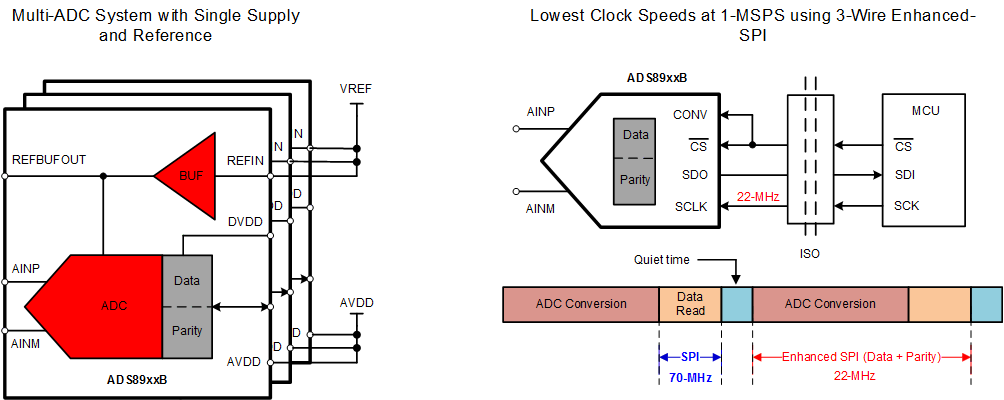
The ADS89xxB boosts analog performance while maintaining high-resolution data transfer by using TI’s Enhanced-SPI feature. Enhanced-SPI enables ADS89xxB in achieving high throughput at lower clock speeds, there by simplifying the board layout and lowering system cost. Enhanced-SPI also simplifies the host’s clocking-in of data there by making it ideal for applications involving FPGAs, DSPs. ADS89xxB is compatible with standard SPI Interface.
The ADS89xxB has an internal data parity feature which can be appended to the ADC data output. ADC data validation by the host, using parity bits, improves system reliability.
SPI Interface Clock at 1 MSPS
| DEVICE RESOLUTION | 3-WIRE SPI | 3-WIRE ENHANCED SPI |
|---|---|---|
| 20 bits | 70 MHz | 22 MHz |
| 18 bits | 58 MHz | 20 MHz |
| 16 bits | 52 MHz | 18 MHz |
- For all features of the enhanced SPI, see the Interface Module section.
